News
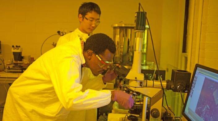
Samwell Emmanuel, S.B. ’17, examines a tiny grid pattern under a microscope in the SEAS teaching clean room. (Photo by Adam Zewe/SEAS Communications.)
A single human hair, barely visible to the naked eye, is about 100 microns in diameter.
That’s huge compared to the device components students build in the Microfabrication Laboratory course at the Harvard John A. Paulson School of Engineering and Applied Sciences (SEAS).Under the instruction of Evelyn Hu, Tarr-Coyne Professor of Applied Physics and of Electrical Engineering, and Peter Stark, Visiting Associate Professor in Engineering Sciences, students are learning the “tricks of the trade” that could enable them to eventually form structures 1,000 times smaller than a strand of hair.
Using a specially designed “teaching clean room” that opened in the SEAS Active Learning Labs last spring, students fabricate electronic and photonic devices, such as light-emitting diodes, by developing components that are so small they must be crafted and analyzed with the help of a microscope.
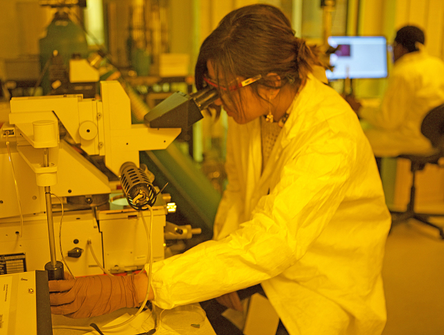
Nabiha Saklayen, a graduate student pursuing a Ph.D. in physics, completes a photolithography workshop in the SEAS teaching clean room. (Photo by Adam Zewe/SEAS Communications.)
Microfabrication involves crafting electronic devices in an unusual way: by printing them onto a material, like silicon. The concept of printed integrated circuits led to a Nobel Prize in physics for electrical engineer Jack Kilby in 2000, and also gave rise to the sophistication and complexity of today’s microprocessors, which can contain more than a billion transistors.
“In order to get a billion transistors into an area that is only an inch or so on a side, obviously you can’t just put the pieces together with your hands,” Hu said. “That set of really intricate techniques is what this course is all about.”
As in printing, shrinking the “font size” allows a tremendously greater amount of information to be represented on the same size page. The economic consequences are enormous, although balanced by the challenges of creating ever-smaller components, Hu explained.
The SEAS teaching clean room provides a first introduction to these techniques, and experience working at larger dimensions with building-block processes and devices. During one afternoon session, students completed a workshop on photolithography, which is a method for transferring a pattern to a substrate. Working at the micron level, they utilized chemicals and UV light to create a metal structure in a grid pattern. They will use this structure in a subsequent lab to measure the flow of electrons.
The course also enables students to work in Harvard’s Center for Nanoscale Systems (CNS), a shared-used core facility that holds a world-class nanofabrication laboratory. Students benefit from the expertise of CNS staff and the guidance of teaching fellows Sarah Schlotter and Laura Adams.
“The students concentrate not only on the fabrication of small devices, which is the main goal of the course, but also how to extract fundamental physical properties from the devices that they fabricate,” said Adams. “Since the course attracts a wide range of concentrators, we like to engage the students at all levels and disciplines to have a really collaborative experimental class.”
For electrical engineering concentrator Samwell Emmanuel, S.B. ’17, it was fascinating to see the tiny pattern take shape.
“We’re used to working with things that we can manipulate with our hands,” he said. “How do you work with something that you can’t even see with the naked eye? That’s what makes this course so interesting to me.”
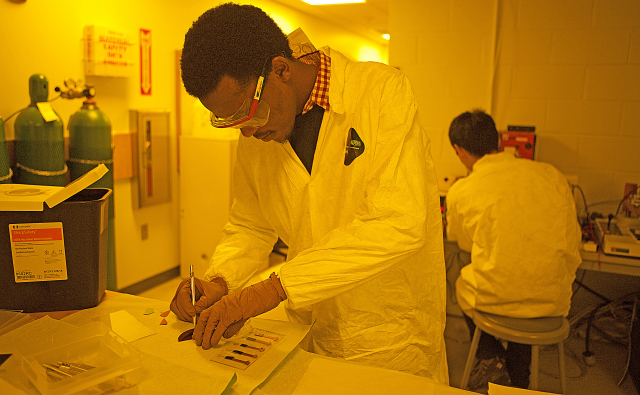
Samwell Emmanuel, S.B. ’17, carefully works with a thin piece of material in the SEAS teaching clean room. (Photo by Adam Zewe/SEAS Communications.)
Nabiha Saklayen, a graduate student pursuing a Ph.D. in physics, enjoyed the opportunity to learn about the fundamental techniques involved in fabricating the kinds of devices she uses regularly for research.
“We usually buy the devices that we need, so these are techniques that we often don’t think about,” she said. “It is incredible how much goes into actually preparing all these different compounds.”
While Hu doesn’t expect students to leave the course with perfect microfabrication skills, she hopes they develop a deeper appreciation for the inevitable challenges of working at the micron-scale.
“That frustration, and the ability to gain insight and intuition from their failures, is a critical thing for the students in this course. I want them to use the imperfections in their devices as a source of feedback to better understand the process,” she said. “My goal is to open their eyes to a world whose features they can’t see. I hope they learn that these techniques are powerful and that they could give them the capability to solve a problem in a different way.”
Cutting-edge science delivered direct to your inbox.
Join the Harvard SEAS mailing list.
Press Contact
Adam Zewe | 617-496-5878 | azewe@seas.harvard.edu