News
Researchers from the Harvard John A. Paulson School of Engineering and Applied Sciences (SEAS) in collaboration with Samsung Advanced Institute of Technology have developed the first neural network for artificial intelligence made using two-dimensional materials. Two-dimensional materials are substances with a thickness of a few nanometers or less, often consisting of a single sheet of atoms. This machine vision processor made from these materials can capture, store and recognize more than 1,000 images.
“This work highlights an unprecedented advance in the functional complexity of 2D electronics,” said Donhee Ham, the Gordon McKay Professor of Electrical Engineering and Applied Physics at SEAS and senior author of the paper. “We have performed both front-end optical image sensing and back-end image recognition in one, 2D, material platform.”
The research was published in Advanced Materials.
This work highlights an unprecedented advance in the functional complexity of 2D electronics.
Since the discovery of graphene in 2004, researchers have been working to harness the unique electronic and optoelectronic properties of atomically thin, two-dimensional semiconductors for the basic building blocks of a range of applications.
Transistors made from two-dimensional materials have been used for simple digital logic circuits and photodetectors but large-scale integration for complex computing, such as artificial intelligence, has remained out of reach. So far, researchers have only been able to integrate about 100 transistors made from two-dimensional materials onto a single chip. To put that in perspective, standard silicon integrated circuits, such as those in your smartphone, contain billions of transistors.
Now, Ham and his team have developed an integrated circuit with more than 1,000 two-dimensional material-based transistors.
“Two-dimensional material-based devices exhibit various exciting properties, but low integration level has restricted their functional complexity,” said Houk Jang, a research associate at SEAS and first author of the paper. “With 1,000 devices integrated on a single chip, our atomically thin network can perform vision recognition tasks, which is a remarkably advanced functionality of two-dimensional material-based electronics.”
The research team used a two-dimensional material called molybdenum disulfide (MoS2), the three-atom thick semiconductor, which interacts well with light. They arranged these photosensitive transistors into what’s known as a crossbar array, which is inspired by neuronal connections in the human brain. This relatively simple set-up allows the device to act as both an eye that can see an image and a brain that can store and recognize an image.
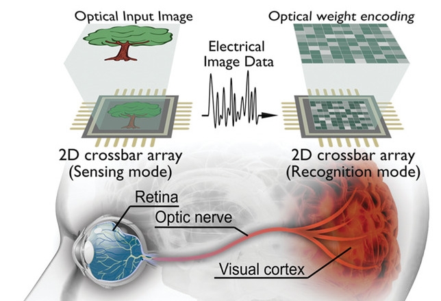
The MoS2 optoelectronic processor mimics two core functions of the human vision system: front‐end image sensing, like the retina and optic nerve, and back‐end recognition, like the brain. (Image courtesy of Houk Jang/Harvard SEAS)
On the front end, the crossbar array acts like an image sensor, capturing an image just like an eye. The photosensitivity of the materials means that the image can be stored and converted into electrical data. On the back end, the same crossbar array can perform networked computing on that electrical data to recognize and identify the image.
To demonstrate the process, the researchers showed the device 1,000 images of handwritten digits. The processor was able to identify the images with 94 percent accuracy.
“Through capturing of optical images into electrical data like the eye and optic nerve, and subsequent recognition of this data like the brain via in-memory computing, our optoelectronic processor emulates the two core functions of human vision,” said Henry Hinton, a graduate student at SEAS and coauthor of the paper.
“This is the first demonstration of a neural network with two-dimensional materials that can interact with light,” said Jang. “Because it computes in memory, you don’t need separate memory and the calculation can be done with very low energy.”
Next, the team aims to scale up the device even further for two-dimensional material-based, high resolution imaging system.
The paper was co-authored by Chengye Liu, Henry Hinton, Min-Hyun Lee, Haeryong Kim, Minsu Seol, Hyeon-Jin Shin and Seongjun Park. It was supported by Samsung Electronics and the National Science Foundation.
Topics: AI / Machine Learning, Applied Physics
Cutting-edge science delivered direct to your inbox.
Join the Harvard SEAS mailing list.
Scientist Profiles

Donhee Ham
John A. and Elizabeth S. Armstrong Professor of Engineering and Applied Sciences
Press Contact
Leah Burrows | 617-496-1351 | lburrows@seas.harvard.edu


