News
Newly discovered atomic vibrations at one of the new interface modes (Credit: NarangLab/Harvard SEAS)
The positions of atoms at the interface between two, 2-D materials control their electronic, magnetic, optical, catalytic, and topological quantum properties but so far, directly measuring these properties has been elusive.
In a recent paper, a collaboration between researchers at UCLA, UC Irvine, and the Harvard John A. Paulson School of Engineering and Applied Sciences measured the exact positions of atoms across an interface between two 2D-materials with picometer precision — about 50 -100 million times smaller than the width of a human hair.
Using a recently developed electron microscopy technique, the researchers were able to build a 3D map of the atoms between these materials and observe for the first time a number of defects, like missing atoms and substitutions of atoms. The researchers used this atomic map as a jumping off point for a new kind of quantum mechanics simulation.

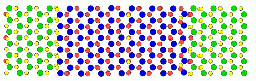
Atomic resolution electron microscopy image of the lateral heterostructure. (Credit: Coherent Imaging Group/UCLA Physics)

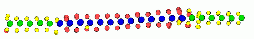
Deformed 'mesh' showing (exaggerated) distortion measured using the exact atomic coordinates (Credit: NarangLab/Harvard SEAS)
The research team, led by Prineha Narang, Assistant Professor of Computational Materials Science at SEAS, tracked the trajectories the atoms took in quantum mechanical simulations and used that information to extract the vibrational modes of the atoms, meaning the periodic motion of atoms in a lattice.
Newly discovered atomic vibrations at one of the new interface modes (Credit: NarangLab/Harvard SEAS)
“We found the interface leads to new vibrational modes which are localized near the interface,” said Georgios Varnavides, a graduate student at SEAS and co-author of the study. “Looking ahead, we know these localized vibrational modes at the interface should lead to an increase in thermal resistance across the interface. Additional calculations and transport measurements of heat across the interface could help us engineer interface thermal resistance, an important current limitation in the design of electronic devices.”
“Our demonstration of the existence of new vibrational modes localized at the interface between two 2D materials, by correlating high-precision atomic measurements and advanced quantum mechanical calculations, could help mitigate the heat dissipation in electronic devices, and increase the lifetime of modern microelectronic devices,” said Narang.
The research was co-authored by Xuezeng Tian, Xingxu Yan, Yakun Yuan, Dennis S. Kim, Christopher J. Ciccarino, Polina Anikeeva, Ming-Yang Li, Lain-Jong Li, Xiaoqing Pan, and Jianwei Miao.
It was primarily supported by the Army Research Office MURI “Ab initio Quantum Materials” program under grant no. W911NF-18-1-0431, the NSF Science and Technology Center under award DMR1548924, and the NSF DMREF program under award DMR-1437263
Topics: Applied Physics, Quantum Engineering
Cutting-edge science delivered direct to your inbox.
Join the Harvard SEAS mailing list.
Press Contact
Leah Burrows | 617-496-1351 | lburrows@seas.harvard.edu


