News
Just about every car, train and plane that’s been built since 1970 has been manufactured using high-power lasers that shoot a continuous beam of light. These lasers are strong enough to cut steel, precise enough to perform surgery, and powerful enough to carry messages into deep space. They are so powerful, in fact, that it’s difficult to engineer resilient and long-lasting components that can control the powerful beams the lasers emit.
Today, most mirrors used to direct the beam in high-power continuous wave (CW) lasers are made by layering thin coatings of materials with different optical properties. But if there is even one, tiny defect in any of the layers, the powerful laser beam will burn through, causing the whole device to fail.
If you could make a mirror out of a single material, it would significantly reduce the likelihood of defects and increase the lifespan of the laser. But what material would be strong enough?
Now, researchers at the Harvard John A. Paulson School of Engineering and Applied Sciences (SEAS) have built a mirror out of one of the strongest materials on the planet: diamond. By etching nanostructures onto the surface of a thin sheet of diamond, the research team built a highly reflective mirror that withstood, without damage, experiments with a 10-kilowatt Navy laser.
"Our one-material mirror approach eliminates the thermal stress issues that are detrimental to conventional mirrors, formed by multi-material stacks, when they are irradiated with large optical powers,” said Marko Loncar, the Tiantsai Lin Professor of Electrical Engineering at SEAS and senior author of the paper. “This approach has potential to improve or create new applications of high-power lasers.”
The research is published in Nature Communications.
Loncar’s Laboratory for Nanoscale Optics originally developed the technique to etch nanoscale structures into diamonds for applications in quantum optics and communications.
“We thought, why not use what we developed for quantum applications and use it for something more classical,” said Haig Atikian, a former graduate student and postdoctoral fellow at SEAS and first author of the paper.
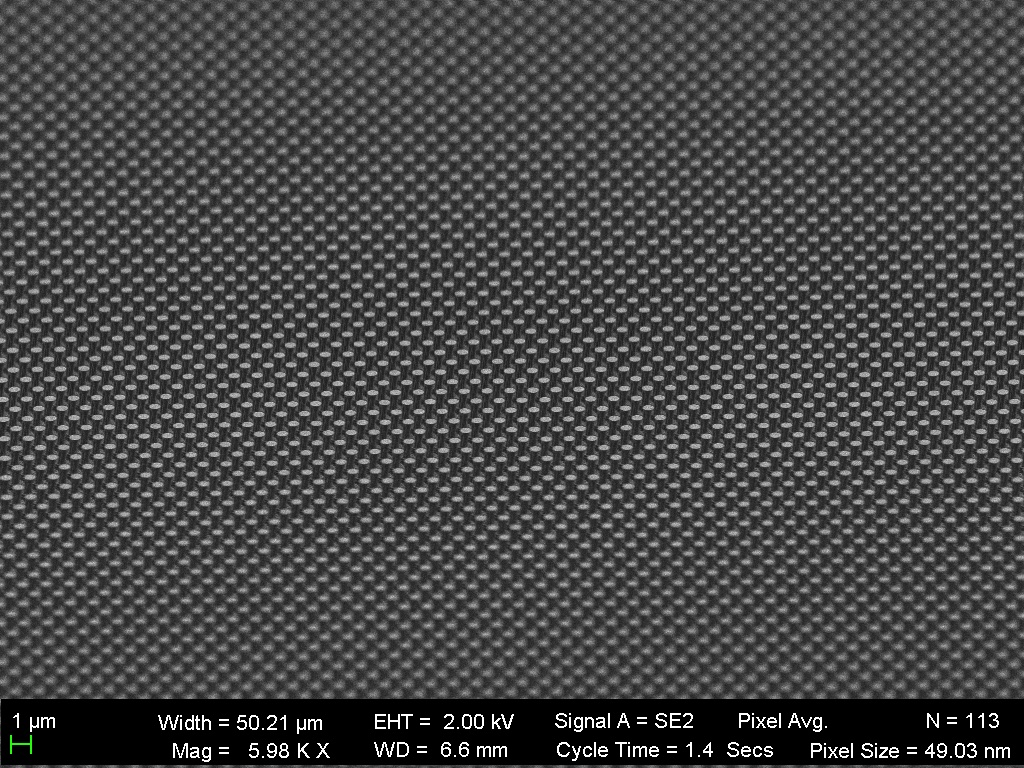
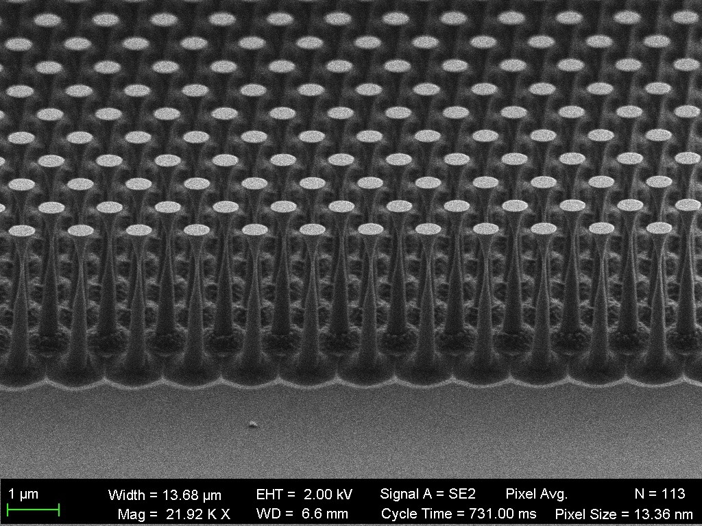
Using this technique, which uses an ion beam to etch the diamond, the researchers sculpted an array of golf-tee shaped columns on the surface on a 3-milimeter by 3-milimeter diamond sheet. The shape of the golf tees, wide on top and skinny on the bottom, makes the surface of the diamond 98.9% reflective.

SEM image of the diamond mirror. (Credit: Loncar Lab/Harvard SEAS)
Download Image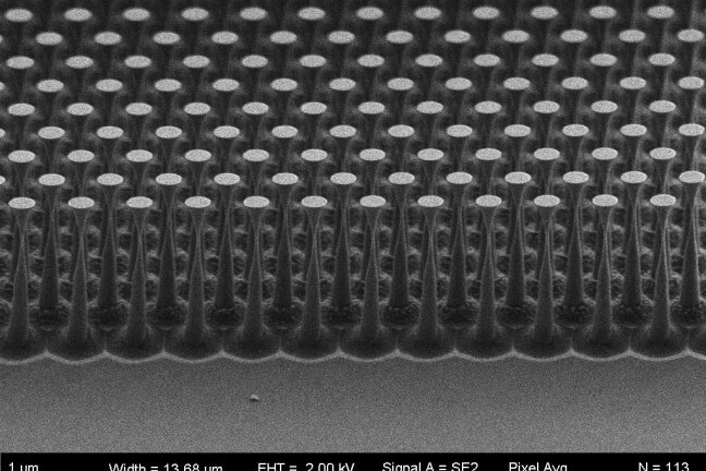
Zoomed SEM image of the mirror (Credit: Loncar Lab/Harvard SEAS)
Download Image“You can make reflectors that are 99.999% reflective but those have 10-20 layers, which is fine for low power laser but certainly wouldn’t be able to withstand high powers,” said Neil Sinclair, a research scientist at SEAS and co-author of the paper.
To test the mirror with a high-power laser, the team turned to collaborators at the Pennsylvania State University Applied Research Laboratory, a Department of Defense designated U.S. Navy University Affiliated Research Center.
There, in a specially designed room that is locked to prevent dangerous levels of laser light from seeping out and blinding or burning those in the adjacent room, the researchers put their mirror in front of a 10-kilowatt laser, strong enough to burn through steel.
The mirror emerged unscathed.
“The selling point with this research is that we had a 10-kilowatt laser focused down into a 750-micron spot on a 3-by-3-millimeter diamond, which is a lot of energy focused down on a very small spot, and we didn’t burn it,” said Atikian. “This is important because as laser systems become more and more power hungry, you need to come up with creative ways to make the optical components more robust.”
In the future, the researchers envision these mirrors being used for defense applications, semiconductor manufacturing, industrial manufacturing, and deep space communications. The approach could also be used in less expensive materials, such as fused silica.
Harvard OTD has protected the intellectual property associated with this project and is exploring the commercialization opportunities.
The research was co-authored by Pawel Latawiec, Xiao Xiong, Srujan Meesala, Scarlett Gauthier, Daniel Wintz, Joseph Randi, David Bernot, Sage DeFrances, Jeffrey Thomas, Michael Roman, Sean Durrant and Federico Capasso, the Robert L. Wallace Professor of Applied Physics and Vinton Hayes Senior Research Fellow in Electrical Engineering at SEAS.
This research was performed in part at the Center for Nanoscale Systems (CNS), a member of the National Nanotechnology Coordinated Infrastructure Network (NNCI), which is supported by the National Science Foundation under NSF award no. 1541959. It was supported in part by the Air Force Office of Scientific Research (MURI, grant FA9550-14-1-0389), the Defense Advanced Research Projects Agency (DARPA, W31P4Q-15-1-0013), STC Center for Integrated Quantum Materials and NSF Grant No. DMR-1231319.
Topics: Applied Physics, Optics / Photonics
Cutting-edge science delivered direct to your inbox.
Join the Harvard SEAS mailing list.
Scientist Profiles

Marko Lončar
Tiantsai Lin Professor of Electrical Engineering
Press Contact
Leah Burrows | 617-496-1351 | lburrows@seas.harvard.edu


