News
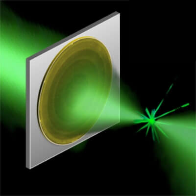
Metasurfaces are a promising type of new nanophotonic technology. A metasurface was recently used at Harvard to create an ultrathin, flat lens that focuses light without imparting the optical distortions of conventional lenses. (Artist's rendition courtesy of Francesco Aieta.)
Cambridge, Mass. – May 1, 2014 – The Air Force Office of Scientific Research has selected the Harvard School of Engineering and Applied Sciences (SEAS) to lead a multidisciplinary effort that will merge research in classical and quantum physics and accelerate the development of advanced optical technologies.
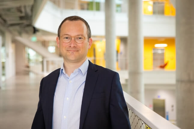
Federico Capasso, Robert L. Wallace Professor of Applied Physics and Vinton Hayes Senior Research Fellow in Electrical Engineering, will lead this Multidisciplinary University Research Initiative with a world-class team of collaborators from Harvard, Columbia University, Purdue University, Stanford University, the University of Pennsylvania, Lund University, and the University of Southampton.
The grant is expected to advance physics and materials science in directions that could lead to very sophisticated lenses, communication technologies, quantum information devices, and imaging technologies.
“This is one of the world’s strongest possible teams,” said Capasso. “I am proud to lead this group of people, who are internationally renowned experts in their fields, and I believe we can really break new ground.”
The premise of nanophotonics is that light can interact with matter in unusual ways when the material incorporates tiny metallic or dielectric features that are separated by a distance shorter than the wavelength of the light. Metamaterials are engineered materials that exploit these phenomena, producing strange effects, enabling light to bend unnaturally, twist into a vortex, or disappear entirely. Yet the fabrication of thick, or bulk, metamaterials—that manipulate light as it passes through the material—has proven very challenging.
Recent research by Capasso and others in the field has demonstrated that with the right device structure, the critical manipulations can actually be confined to the very surface of the material—what they have dubbed a “metasurface.” These metasurfaces can impart an instantaneous shift in the phase, amplitude, and polarization of light, effectively controlling optical properties on demand. Importantly, they can be created in the lab using fairly common fabrication techniques.
At Harvard, the research has produced devices like an extremely thin, flat lens, and a material that absorbs 99.75% of infrared light. But, so far, such devices have been built to order—brilliantly suited to a single task, but not tunable.
“Can we make a rapidly configurable metasurface so that we can change it in real time and quickly? That’s really a visionary frontier,” said Capasso. “We want to go all the way from the fundamental physics to the material building blocks and then the actual devices, to arrive at some sort of system demonstration.”
The proposed research also goes further. A key thrust of the project involves combining nanophotonics with research in quantum photonics. By exploiting the quantum effects of luminescent atomic impurities in diamond, for example, physicists and engineers have shown that light can be captured, stored, manipulated, and emitted as a controlled stream of single photons. These types of devices are essential building blocks for the realization of secure quantum communication systems and quantum computers. By coupling these quantum systems with metasurfaces—creating so-called quantum metasurfaces—the team believes it is possible to achieve an unprecedented level of control over the emission of photons.
“Just 20 years ago, the notion that photons could be manipulated at the subwavelength scale was thought to be some exotic thing, far fetched and of very limited use,” said Capasso. “But basic research opens up new avenues. In hindsight we know that new discoveries tend to lead to other technology developments in unexpected ways.”
The research team includes experts in theoretical physics, metamaterials, nanophotonic circuitry, quantum devices, plasmonics, nanofabrication, and computational modeling. Co-principal investigator Marko Lončar is the Tiantsai Lin Professor of Electrical Engineering at Harvard SEAS. Co-PI Nanfang Yu, Ph.D. ’09, developed expertise in metasurfaces as a student in Capasso’s Harvard laboratory; he is now an assistant professor of applied physics at Columbia. Additional co-PIs include Alexandra Boltasseva and Vladimir Shalaev at Purdue, Mark Brongersma at Stanford, and Nader Engheta at the University of Pennsylvania. Lars Samuelson (Lund University) and Nikolay Zheludev (University of Southampton) will also participate.
The bulk of the funding will support talented graduate students at the lead institutions.
The project, titled “Active Metasurfaces for Advanced Wavefront Engineering and Waveguiding,” is among 24 planned MURI awards selected from 361 white papers and 88 detailed proposals evaluated by a panel of experts; each award is subject to successful negotiation. The anticipated amount of the Harvard-led grant is up to $6.5 million for three to five years.
Harvard SEAS will also participate in a second MURI, the Department of Defense has announced. Efthimios Kaxiras, John Hasbrouck Van Vleck Professor of Pure and Applied Physics, is a co-principal investigator on a team of physicists, chemists, mathematicians, computational scientists, and materials scientists who will use multiscale modeling to predict and design new functional materials. That project will be led by Mitchell Luskin at the University of Minnesota.
Topics: Optics / Photonics, Electrical & Computer Engineering, Awards, Applied Physics
Cutting-edge science delivered direct to your inbox.
Join the Harvard SEAS mailing list.
Scientist Profiles

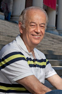
Marko Lončar
Tiantsai Lin Professor of Electrical Engineering
Federico Capasso
Robert L. Wallace Professor of Applied Physics and Vinton Hayes Senior Research Fellow in Electrical Engineering